Impact Factor
7.883
Call For Paper
Volume 12 Issue 09
September 2026
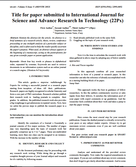
Download Paper Format
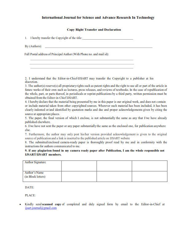
Copyright Form

Author(s)
Mr. Jayant Thadani Dr. P. M. Daigavane Dr. D. R. Tutakne
Abstract
A Three Level Two Switch Inverter With Step Up Transformer And A Suitable LC Component System Is Employed. The Output Of This Scheme Is In Quasi Square Wave Form, Which Is Then Converted To Regulated Sine Wave Output By Use Of LC Component. The System
Keywords
Sine Wave Output
Grid Synchronization
Phase Angle Control
3 Level Inverter
Paper ID
IJSARTV3I38715
Publication Date
March 29, 2017
Research Area
Electrical Engineering