Impact Factor
7.883
Call For Paper
Volume 12 Issue 07
July 2026
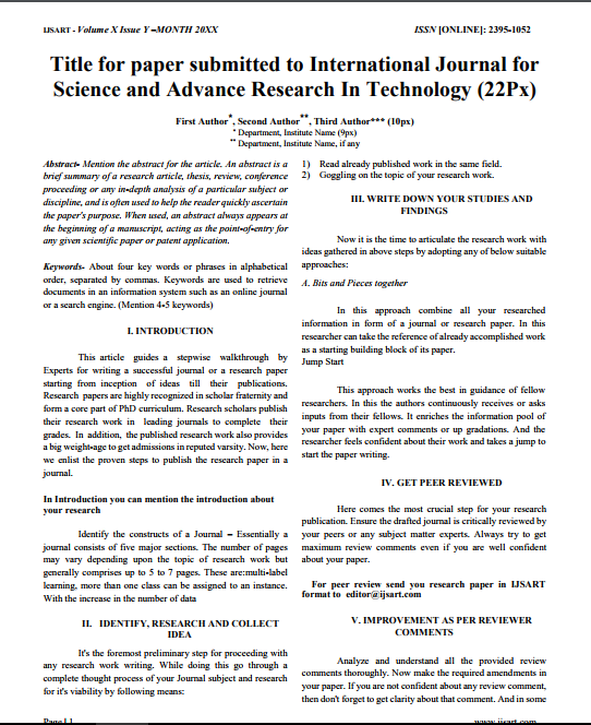
Download Paper Format
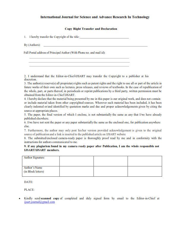
Copyright Form

Author(s)
M.Gayathri R.Jamuna
Abstract
This Paper Presents A New Design Of A 2 To 4 Decoder Constructed Using 3-transistor NAND Gates, Contrasting It With The Conventional 4 Transistor NAND Gate-based Technique. The Primary Aim Of This Paper Is To Exhibit Advancements In Power Efficiency, Worst-case Propagation Time Delay, And Power Delay Product (PDP). These Improvements Underscore The Efficacy Of The 3-transistor NAND Gate-based Design, Illustrating Its Potential For Efficient And Optimized Decoder Architectures. The Simulation Of The Design Is Carried Out Using SPICE With 250nm Technology.
Keywords
CMOS
Delay
Low Power
NAND
PDP
VLSI.
Paper ID
IJSARTV11I4102967
Publication Date
April 1, 2025
Research Area
ECE