Impact Factor
Call For Paper
Volume 12 Issue 08
August 2026
Download Paper Format
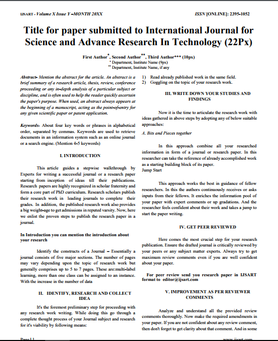
Copyright Form
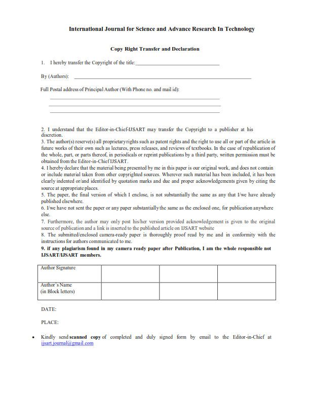

Author(s)
Abstract
Machine Learning Methods Are Not Much Applied In The PCB Defect Detection Process. Modern World Is More Adapted To Machine Learning And Artificial Intelligent Applications. Many Other Sectors Were Already Using Applications Based On These Technologies. A Printed Circuit Board Or (PCB) Is Used To Physically Support And Realistically Connect Electronic Components Using Conductive Pathways, Track Or Signal Traces Etched From Copper Sheets Laminated Onto A Conductive Substrate. The Self Inspection Of PCBs Serves A Purpose Which Is Traditional In Modern Technology. The Aim Is To Relieve Human Inspectors Of The Tedious And Inefficient Task Of Looking For Those Defects In PCBs Which Could Lead To Electric Failure. We First Compare A PCB Standard Image With A PCB Image, Using A Simple Subtraction Algorithm That Can Highlight The Main Problem-regions. We Have Also Seen The Effect Of Noise In A PCB Image That At What Level This Method Is Suitable To Detect The Faulty Image. Finally, Defect Classification Operation Is Employed In Order To Identify The Source For Six Types Of Defects Namely, Missing Hole, Pin Hole, Under Etch, Short-circuit, Mouse Bite, And Open-circuit.
Keywords
Paper ID
IJSARTV12I8105823
Publication Date
August 15, 2026
Research Area
Electronics And Communication