Impact Factor
Call For Paper
Volume 12 Issue 07
July 2026
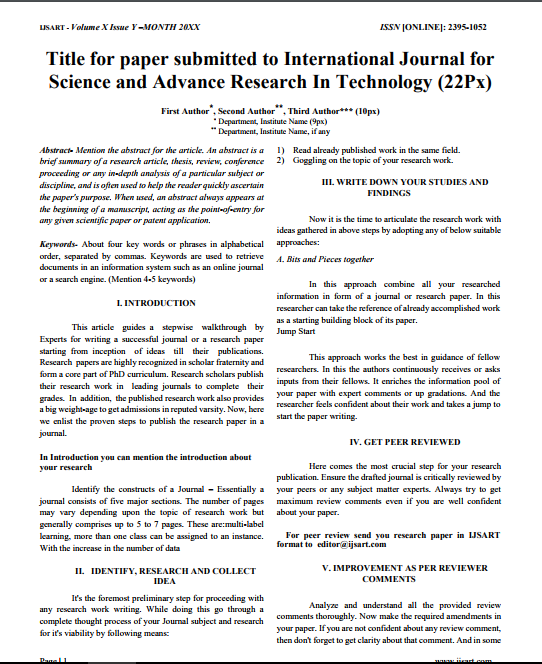
Download Paper Format
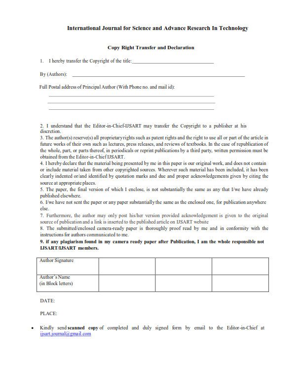
Copyright Form

Author(s)
Abstract
In The Fast-paced Electronics Manufacturing Industry, Ensuring Printed Circuit Board (PCB) Quality Is Vital For Producing Reliable, High-performance Devices. Traditional Methods Like Manual Inspection And Rule-based Vision Struggle With Small Or Complex Defects, Leading To Inefficiencies. This Work Presents A Deep Learning-based Approach Using YOLOv8 For Automated PCB Defect Detection And Classification. The System Detects Defects Such As Missing Holes, Mouse Bites, Open Circuits, Shorts, Spurious Copper, And Spurs With Real-time Performance And Achieves A Mean Average Precision (mAP) Above 90%. Integrated With A Flask Web Application, It Allows Instant PCB Image Analysis, Offering A Scalable And Efficient Solution For Quality Control.The Use Of YOLOv8 Ensures Fast Inference Speed, Making The System Suitable For Real-time Deployment In Production Lines. The Model Is Trained On A Diverse Dataset Of PCB Images, Improving Its Robustness Against Variations In Defect Type, Size, And Position. By Automating The Defect Detection Process, The System Reduces Dependency On Manual Labor And Minimizes Inspection Errors. It Also Provides Manufacturers With A Cost-effective Solution That Scales With Industry Demands. Future Improvements Will Target Multi-layer PCB Inspection, Advanced Imaging (X-ray/IR), Predictive Maintenance, And Edge-based Inference, Making It Adaptable To Next-generation Electronics Manufacturing.
Keywords
Paper ID
IJSARTV11I9104012
Publication Date
September 12, 2025
Research Area
Electronics Engineering