Impact Factor
7.883
Call For Paper
Volume 12 Issue 09
September 2026
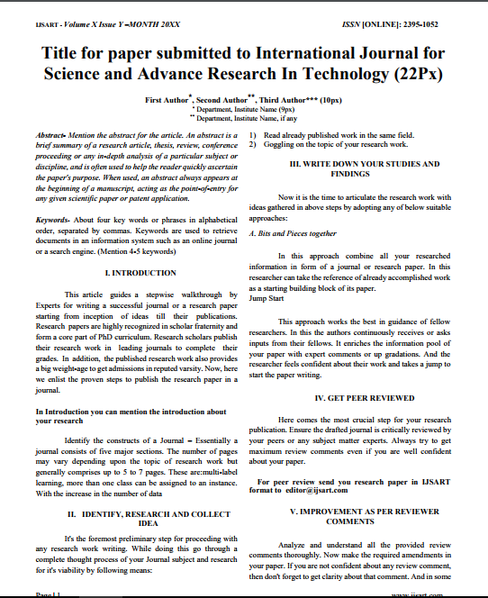
Download Paper Format
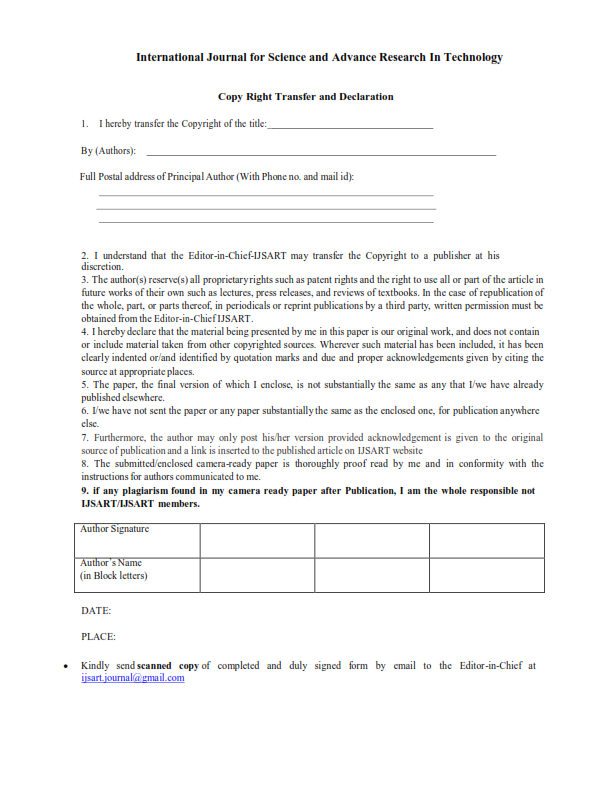
Copyright Form

Author(s)
Saumya Paliwal Shivani Saxena
Abstract
GaN Materials Are Increasingly Becoming Popular As A Replacement To The Si Based Devices. Due To Their Wide Band Gap They Have A Huge Potential For High Power And High Frequency Applications In The Field Of Military, Satellite, Led’s, Lasers, Medicine And
Keywords
Gallium Nitride
MOS HEMT Device
Wideband Gap
2DEG.
Paper ID
IJSARTV5I229387
Publication Date
February 17, 2019
Research Area
Electronics